| Qty | Component | Components | Comment | Location |
| 1 | PCB | |||
| 2 | 27pF | C1 2 | under main chip | |
| 2(4) | 0.01uF | C11 C11b | centre and lower right and next to the IGN FETs |
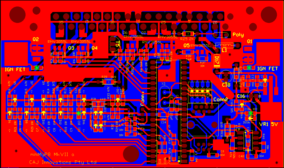 |
| 2 | 1.0uF | C12 C12b | centre and right |
 |
| 6 | 56R | R5 6 7 8 28 38 | top |
 |
| 2 | 1K5 | R26 27 | left centre |
 |
| 2 | 2K7 | R25 34 | under main chip and top |
 |
| 1 | 3K3 | R35 | under chip |
 |
| 2 | 3K9 | R29 R29b | top centre,right |
 |
| 2 | 6K8 | R31 R31b | centre, right |
 |
| 14 | 10K | R1-4 17 17b 18-21 24 28g 37 40 | mainly centre left or near FETs |
 |
| 12 | 47k | R12 12b 13-16, 22, 23, 32 32b 33 33b | mainly centre left, two lower right |
 |
| 1 | 100uF 25V | C18 | upper right | Caution, must go correct way |
| 13 | 100nF (104) | All other caps |
 |
|
| 1 | 100uH | L1 | upper right | |
| 1 | IN5819 | D17 | upper right | Caution, must go correct way |
| 18 | IN914 | All other diodes | Any general purpose small signal diode | Caution, must go correct way |
| 1 | BC547 | T5 | top centre | Caution, must go correct way |
| 0(2) | IGBT 430V | Q1-2 | logical level IGN FET | |
| 2 | VND10N06 | Q3-4 | 60V 10A logical level FET | |
| 4(2) | RNV3055L | Q1,2,5,6 | 60V 3A logical level FET | |
| 1 | LM7805 | surface mount | ||
| 1 | 8Mhz XTAL | X1 | ||
| 1 | RJ45 connector | |||
| 1 | 4 DIP switch | |||
| 1 | 6 pin header | for firmware upgrades | ||
| 1 | 3pin header | for o2 sensor inputs | ||
| 1 | Polyswitch | upper right | looks like yellow disc capacitor | |
| 1 | MOV | small dark surface mount | better to mount directly under main connector between pins 19 and 20 | |
| 1 | 40 pin IC socket | Caution, must go correct way | ||
| 1 | 8 pin IC socket | Caution, must go correct way | ||
| 1 | Atmega324 | Caution, must go correct way | ||
| 1 | Attiny25 | Caution, must go correct way |
Assembly
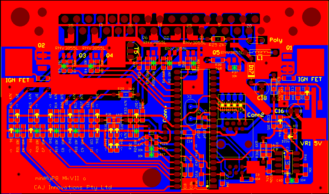
All the images can be clicked to reveal a higher resolution image. For the part locator image, look for the green stars.
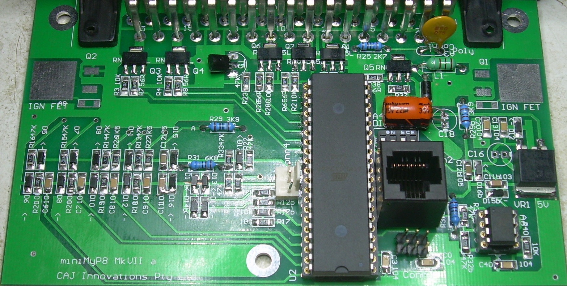
This kit contains many small components. A clear workspace is recommended. First identify the all components. Use the parts count to help. All the resistors are clearly labelled but the surface mount capacitors are unmarked. Construction should only be attempted by experienced hobbyists.
A small soldering iron and tweezers are required and a visual aid like a lit magnifying glass is recommended. There are also some parts ( the FET bodies, some ground connections and the main connector ) that will require a soldering iron that has a higher heat capacity ( not termperature ) to properly heat the solder.
I suggest assembly in the order of the parts list ( left ) upto and including the MOV( apply MOV with main connector ). Don't solder in Q5 yet.
Important Errata:
For the version driving the coils directly, The driver FETs are only partially integrated. Only their source pin is grounded. The gate and drain pins must be wired to the smaller Q1, Q2 pads. Also it is important that the ECU's output polarity is reversed in this configuration. This is done by grounding pin 1 ( lower right ) of the main chip with a wire.
Testing
Make sure the two chips are not in their socket and Q5 not installed for these initial tests. I suggest using a small 9V battery or a 12V battery with a 100 ohm resistor in series. Do not proceed if a test fails.
- Apply the negative of the voltage source to one of the mounting holes.
- Apply the positive to the top leg of the polyswitch or pin 20 of the main connector.
- Check that nothing is getting warm ( including the series resistor if used ). The voltage drop across polyswitch should be less than 1/2 volt.
- Check for most of the voltage at the right pin of the voltage regulator (closest to edge ). Expect greater than 7V
- There should be 5V on pins 10,30,32 of the 40 pin socket. If you are seeing higher you may have D12 ( near regulator ) the wrong way.
- Pin 4 should be 2.5V and pin 3 should be 2.7V.
- If everything above has checked out remove the power and insert the chips the correct way. Now recheck the previous steps
- Set the 4 way switch to On, Off, Off, Off
At this stage you need to get the MyECU talking to the PC or Android device. To contruct the bluetooth dongle get the instructions from here. The latest Android Optimiser and manual can be found here
- Disconnect the power and connect the bluetooth dongle to MyECU using the network cable.
- Apply power to MyECU without the series resistor if previously used. You should now see a red flashing LED on the dongle. Start the Android Optimiser and connect to the BT dongle. It will probably ask for a PIN. Use 1234. When successfully connected the green LED should light. The temperature analogs should be at full scale, the voltage should display correctly. They others will float around 1/2 scale.
- You should see a 10V square wave on the low leg of R25 ( the tacho signal )
- Check the voltage at the lower leg of R28. You should see it go to 5V for 2 seconds after connecting power. Check that the gates of the 4 FETs(leftmost pin) Q1 and 2 are at 5V, all others at 0V
- Now double check your handywork and fit the PCB into the case and connect the ECU to the bike. It would be best to have the ECUController or Optimiser connected.We ARE NOT going to try to start the bike yet. Being careful to monitor for smoke or heat, turn on the ignition. You should hear the fuel pump turn for 2 seconds.The tacho my vibrate a little. Check all the analogs with the Android Optimiser. They should all be correct and the throttle should be tracked.
- Well done, at this stage construction is nearly complete. You can add Q5. Proceed to the "First steps" page