Errata
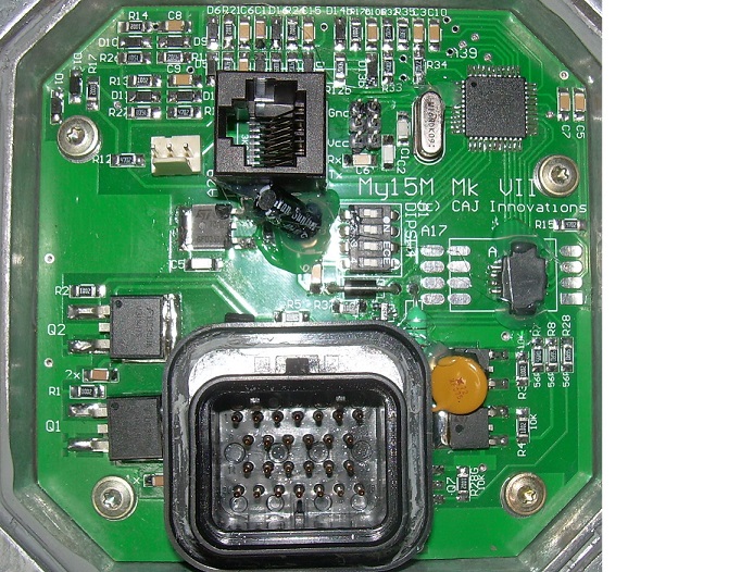
The latest board has some circuit enhancement around Q5 and some minor variation to that picture.
Solder C18 early as it needs good access.
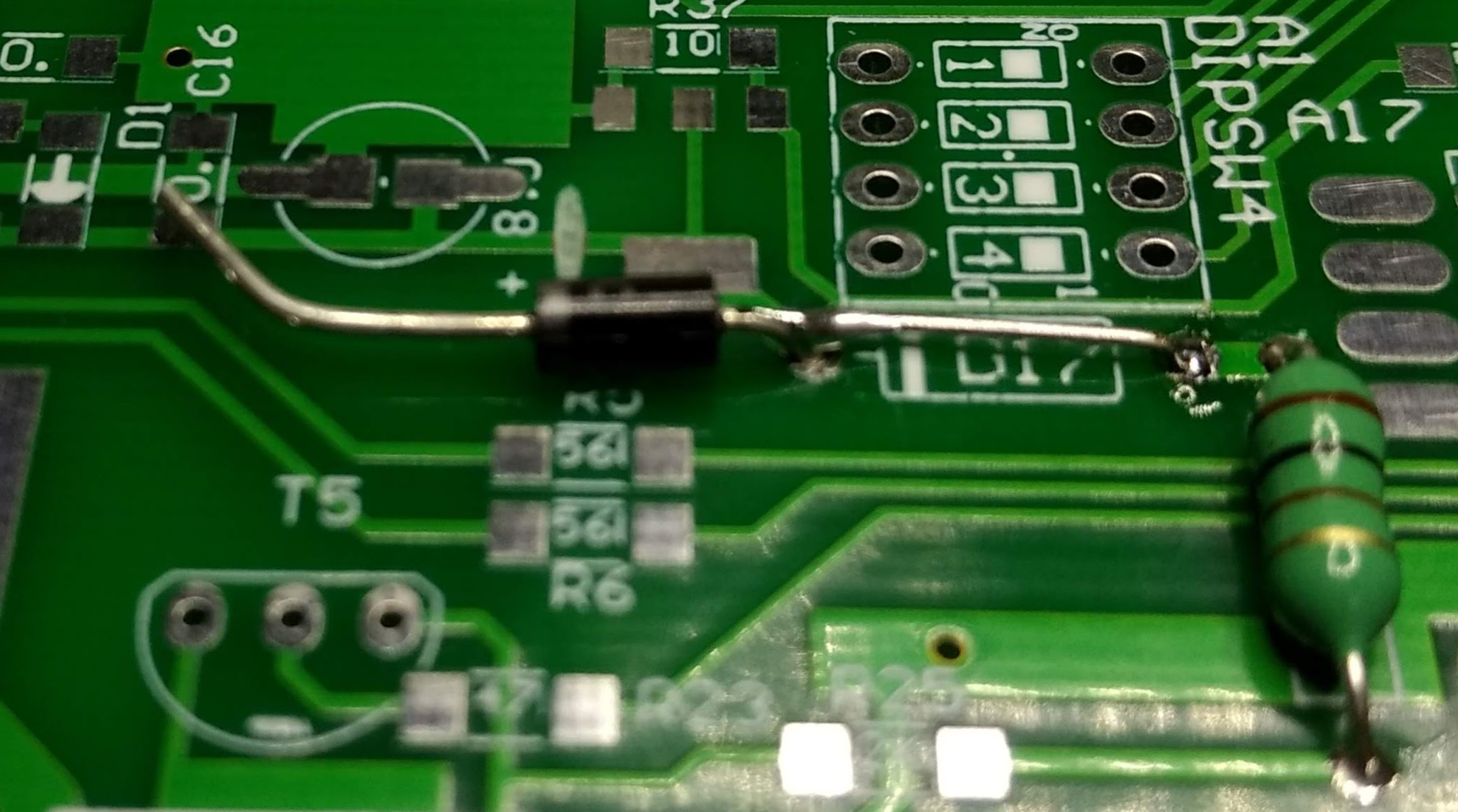
D17 does not go in its marked spot due to error in the board. It goes to the left with its right leg in the left hole and the left leg connected to C16 lower pad. Install a link where D17 should of gone. See pic below.

Assembly
Construction should only be attempted by experienced hobbyists. This kit contains many small components. A clear workspace is recommended. First identify the all components. Use the parts count to help. All the resistors are clearly labelled but the surface mount capacitors are unmarked as is the MOV.
A small soldering iron and tweezers are required and a visual aid like a lit magnifying glass is recommended. There are also some parts ( the FET bodies, some ground connections and the main connector ) that may require a soldering iron that has a higher heat capacity ( not termperature ) to properly heat the solder.
First you need to determine what variant of 15M you have. There are two types I've come across but only one particular Ducati was of the 2nd type. You'll notice that near Q7 there are two tabs. The most common type drives the fuel pump with pin 19, For this you need to jumper the right pad to the lower pad. The other type drives the fuel pump on pin 15 so you need to jumper the right pad to the upper pad. For this 2nd type also you will need to earth pin 19 ( You can jumper the lower left pad to the gnd pin of Q7).
I suggest assembly in the order of the parts list ( left ) upto and including the MOV. For the MOV, use a couple of wire lead offcuts ( These can be used to apply power for testing so leave a bit of over hang). Position MOV fully against the upper wire to improve clearance from the earth PCB. Bend the lower wire towards the MOV. Then refer to testing to complete the kit. Note some components around the ignition FETs (R1 and R2 ) are not used.
Tips: For the resistors/capacitors I put a small dab of solder on one PCB pad first. Then position the component and then apply heat to that side, Try and keep the tip flush with the body of the component. Keep time short. The capacitors seem sensitive to too much heat as there have been a few failure of them.
Testing
Make sure R38 not installed for these initial tests. I suggest initially using a small 9V battery or a 12V battery with a 100 ohm resistor in series. Do not proceed if a test fails.
Double check the orientation of D1 near the voltage regualtor. If wrong it will allow close to the battery voltage to reach the chip. That will not end well. Probably best to read the entire test steps first before trying them.
- Apply the negative of the voltage source to one of the mounting holes or the lower hook of the MOV.
- Apply the positive to upper hook on the Mov or the lower leg of the polyswitch.
- Check that nothing is getting warm ( including the series resistor if used ). The voltage drop across polyswitch should be less than 1/2 volt.
- Check for most of the voltage at the lower pin of the voltage regulator. Expect greater than 7V
- There should be 5V on the upper pin of the regulator. If you are seeing higher you may have D1 the wrong way.
- Top right of the board. The common junction between R32/R33 should be 2.5V and lower pin of R35 should be 2.7V.
- Check that the gates of the 5 FETs ( look for the tracks coming from the 56R resistors ) are all at 0V. You should see the gate on Q7 ( fuel pump prime ) go to 5V for 1 to 2 seconds at power up
At this stage you need to get the MyECU talking to the PC or Android device. Refer to the Andoid Optimiser or ECUController manual for the steps required to estasblish communicatioon with the MyECU.
- The two temperature should appear at -30C and the battery voltage should be correct. The other inputs will float randomly
- Now double check your handywork and fit the PCB into the case and connect the ECU to the bike.Set all switches off except SW1. It would be best to have the ECUController or Optimiser connected.We ARE NOT going to try to start the bike yet. Being careful to monitor for smoke or heat, turn on the ignition. You should hear the fuel pump turn for 2 seconds.The tacho my vibrate a little.Check the analogs with the ECUController or Optimiser. They should all be correct and the throttle should be tracked.
- Well done, at this stage construction is complete. Proceed to the "First steps" page


